Home / ECE / Electronic Devices and Circuits :: Section 4

ECE :: Electronic Devices and Circuits

  1. An increase in junction temperature of a semiconductor diode

  2. A.
    causes a small increase in reverse saturation current
    B.
    causes a large increase in reverse saturation current
    C.
    does not affect reverse saturation current
    D.
    may cause an increase or decrease in reverse saturation current depending on rating of diode

  3. An air gap provided in the iron core of an inductor prevents

  4. A.
    flux leakage
    B.
    hysteresis loss
    C.
    core saturation
    D.
    heat generation

  5. Generally, the gain of a transistor amplifier falls at high frequency due to the

  6. A.
    internal capacitance of the device
    B.
    coupling capacitor at the I/P
    C.
    skin effect
    D.
    coupling capacitor at the O/P

  7. Which of these has a layer of intrinsic semiconductor?

  8. A.
    Zener diode
    B.
    PIN diode
    C.
    Photo diode
    D.
    Schottky diode

  9. Assertion (A): When Diode used as rectifier the reverse breakdown voltage should not be exceeded.

    Reason (R): A high inverse voltage can destroy a p-n junction.

  10. A.
    Both A and R are true and R is correct explanation of A
    B.
    Both A and R are true but R is not a correct explanation of A
    C.
    A is true but R is false
    D.
    A is false but R is true

  11. A Si sample is doped with a fixed number of group N impurities. The electron density n is measured from 4 K to 1200 k for the sample. Which one of the following is correct?

  12. A.
    n remains constant over the temperature range
    B.
    n increases monotonicaliy with increasing temp
    C.
    n increases first remains constant over a range and again increases with increasing temperature
    D.
    n increases show a peak and then decrease with temperature

  13. Assertion (A): In design of circuit using BJT, a derating factor is used.

    Reason (R): As the ambient temperature increases, heat dissipation becomes slower.

  14. A.
    Both A and R are true and R is correct explanation of A
    B.
    Both A and R are true but R is not a correct explanation of A
    C.
    A is true but R is false
    D.
    A is false but R is true

  15. If the drift velocity of holes under a field gradient of 100 V/m is 5m/sec. Their mobility is

  16. A.
    0.05
    B.
    0.5
    C.
    50
    D.
    500

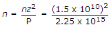
  17. In a P type silicon sample, the hole concentration is 2.25 x 10¹⁵ / cm3. If the intrinsic carrier concentration is 1.5 x 10¹⁰/ cm3 the electron concentration is

  18. A.
    zero
    B.
    1010/cm3
    C.
    105/cm3
    D.
    1.5 x 1025/cm3

  19. The behaviour of a JFET is similar to that of

  20. A.
    NPN transistor
    B.
    PNP transistor
    C.
    SCR
    D.
    Vacuum triode