ECE :: Electronic Devices and Circuits
-
Determine the transistor capacitance of a diffused junction varicap diode of a reverse potential of 4.2 V if C(0) = 80 pf and VT = 0.7 V
-
The cut in voltage of a diode is nearly equal to
-
Assertion (A): In a BJT base current is very small.
Reason (R): In a BJT recombination in base region is high.
-
A reverse voltage of 18 V is applied to a semiconductor diode. The voltage across the depletion layer is
-
Assertion (A): Germanium is more commonly used than silicon.
Reason (R): Forbidden gap in germanium is less than that in silicon.
-
Which of the following devices has substrate?
-
Assertion (A): The amount of photoelectric emission depends on the intensity of incident light.
Reason (R): Photo electric emission can occur only if frequency of incident light is less than threshold frequency.
-
In degenerate p type semiconductor material, the Fermi level,

 Whatsapp
 Facebook


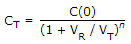 , Here n =
  for diffused junction
 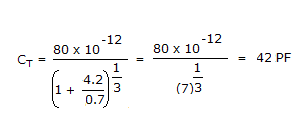 .
.