Home / ECE / Electronic Devices and Circuits :: Section 11

ECE :: Electronic Devices and Circuits

  1. The depletion layer in a reverse biased p-n junction is due to the presence of

  2. A.
    electrons
    B.
    holes
    C.
    both electrons and holes
    D.
    immobile ions

  3. Which materials find application in MASER?

  4. A.
    Diamagnetic
    B.
    Paramagnetic
    C.
    Ferromagnetic
    D.
    Ferrimagnetic

  5. An electrically neutral semiconductor has

  6. A.
    no free charges
    B.
    no majority carriers
    C.
    no minority carriers
    D.
    equal number of positive and negative charges

  7. Magnetic recording tape is most commonly made from

  8. A.
    small particles of iron
    B.
    silicon iron
    C.
    ferric-oxide
    D.
    silver nitrate

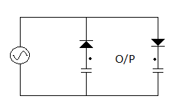
  9. The circuit shown in the figure is best described as a

  10. A.
    bridge rectifier
    B.
    ring modulator
    C.
    frequency discriminator
    D.
    voltage doubler

  11. Gold is often diffused into silicon P-N junction devices to

  12. A.
    increase recombination rate
    B.
    reduce recombination rate
    C.
    make silicon a direct gap semiconductor
    D.
    make silicon semimetal

  13. In a solar cell, the photovoltaic voltages is the voltage at which the resultant current is

  14. A.
    positive
    B.
    zero
    C.
    negative
    D.
    rated current

  15. The forbidden energy gap between the valence band and conduction band will be wide in case of

  16. A.
    semiconductors
    B.
    all metals
    C.
    good conductors of electricity
    D.
    insulators

  17. At 0 K the forbidden energy gap in intrinsic semi conductor is about

  18. A.
    10 eV
    B.
    6 eV
    C.
    1 eV
    D.
    0.2 eV

  19. The resistance of a metallic wire would

  20. A.
    increase as the operating frequency increase
    B.
    decrease as the operating frequency increase
    C.
    remain unaffected on increasing the operating frequency
    D.
    first increase then decrease