ECE :: Electronic Devices and Circuits
-
An incremental model of a solid state device is one which represents the
-
What is the correct sequence of the following step in the fabrication of a monolithic, Bipolar junction transistor?
- Emitter diffusion
- Base diffusion
- Buried layer formation
- E pi-layer formation
-
For an n-channel enhancement type MOSFET, if the source is connected at a higher potential than that of the bulk (VSB > 0), the threshold voltage VT of the MOSFET will
-
Which of the following is used for generating time varying wave forms?
-
Calculate the resistivity of n-type semiconductor from the following data, Density of holes = 5 x 1012 cm-3. Density of electrons = 8 x 1013 cm-3, mobility of conduction electron = 2.3 x 104 cm2/ V-sec and mobility of holes = 100 cm2/V-sec.
-
An one sided abrupt junction has 1021/m3 of dopants on the lightly doped side, zero bias voltage and a built-in potential of 0.2 V. The depletion width of abrupt junction.(q = 1.6 x 10⁻¹⁹ C, εr =16, ε0 = 8.87 x 10⁻¹² F/m) is
-
n-type semiconductors
-
In all metals
-
The voltage across a zener diode
-
Assertion (A): Two transistors one n-p-n and the other p-n-p are identical in all respects (doping, construction, shape, size). The n-p-n transistor will have better frequency response.
Reason (R): The electron mobility is higher than hole mobility.

 Whatsapp
 Facebook


 .
.  σ = e(neue + nnun).
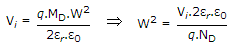 .
.