Home / ECE / Electronic Devices and Circuits :: Section 8

ECE :: Electronic Devices and Circuits

  1. Assertion (A): Hall effect is used to find the type of semiconductor.

    Reason (R): When a specimen of semiconductor carrying current I lies in a magnetic field the force on electrons and holes is in opposite directions.

  2. A.
    Both A and R are true and R is correct explanation of A
    B.
    Both A and R are true but R is not a correct explanation of A
    C.
    A is true but R is false
    D.
    A is false but R is true

  3. The fT of a BJT is related to its gm, Cp and Cμ as follows.


  4. When a p-n junction is forward biased. The width of depletion layer decreases.

  5. A.
    True
    B.
    False

  6. In which of the following case the rating of the transformer to deliver 100 watts of d.c. power to a load, will be least?

  7. A.
    Half wave rectifier
    B.
    Full wave rectifier
    C.
    Bridge type full wave rectifier
    D.
    Three phase full wave rectifier

  8. When a p-n Junction is forward biased

  9. A.
    the current flow is due to electrons only
    B.
    the majority carriers in both p and n materials are driven toward the junction.
    C.
    the majority carriers in both p and n materials are away from the junction.
    D.
    both (a) and (c).

  10. In a JFET, the drain current is maximum when

  11. A.
    VGS = 0
    B.
    VGS is not zero but is slightly negative
    C.
    VGS is negative
    D.
    VGS is negative and equal to VDS

  12. A potential difference is developed across a current carrying metal strip when the strip is placed in a transverse magnetic field. The above effect is known as

  13. A.
    Fermi's effect
    B.
    Photo electric effect
    C.
    Joule's effect
    D.
    Hall's effect

  14. In a zener diode

  15. A.
    forward voltage rating is high
    B.
    negative resistance characteristics exists
    C.
    sharp breakdown occurs at low reverse voltage
    D.
    none of the above

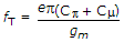
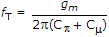
  16. Which one of the following bipolar transistors has the highest current gain bandwidth Product (fr) for similar geometry?

  17. A.
    NPN germanium transistor
    B.
    NPN silicon transistor
    C.
    PNP germanium transistor
    D.
    PNP silicon transistor

  18. The depletion layer across a P+ n junction lies

  19. A.
    mostly in the P+ region
    B.
    mostly in n region
    C.
    equally in both the P+ and n-region
    D.
    entirely in the P+ region