ECE :: Electronic Devices and Circuits
-
At room temperature the current in an intrinsic semiconductor is due to
-
Work function is the maximum energy required by the fastest electron at 0 K to escape from the metal surface.
-
The most commonly used semiconductor material is
-
In which of these is reverse recovery time nearly zero?
-
A transistor has a current gain of 0.99 in the CB mode. Its current gain in the CC mode is
-
In p-n-p transistor the current IE has two components viz. IEP due to injection of holes from p-region to n-region and IE due to injection of electrons from n-region to p-region. Then
-
The amount of photoelectric emission current depends on
-
Assertion (A): A p-n junction has high resistance in reverse direction.
Reason (R): When a reverse bias is applied to p-n junction, the width of depletion layer increases.
-
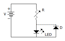
In the circuit of figure the function of resistor R and diode D are

 Whatsapp
 Facebook


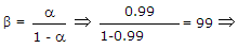 Current gain = 1 + β = 100.