Home / ECE / Electronic Devices and Circuits :: Section 1

ECE :: Electronic Devices and Circuits

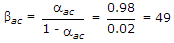
  1. An amplifier without feedback has a voltage gain of 50, input resistance of 1 kΩ and output resistance of 2.5 kΩ. The input resistance of the current shunt -ve feedback amplifier using the above amplifier with a feedback factor of 0.2 is

  2. A.
    1/11 kΩ
    B.
    1/5 kΩ
    C.
    5 kW
    D.
    11 kW

  3. As compared to an ordinary semiconductor diode, a Schottky diode

  4. A.
    has lower cut in voltage
    B.
    has higher cut in voltage
    C.
    lower reverse saturation current
    D.
    both (b) and (c)

  5. Assertion (A): When a high reverse voltage is applied to a p-n junction the diode breaks down.

    Reason (R): High reverse voltage causes Avalanche effect.

  6. A.
    Both A and R are true and R is correct explanation of A
    B.
    Both A and R are true but R is not a correct explanation of A
    C.
    A is true but R is false
    D.
    A is false but R is true

  7. As compared to an ordinary semiconductor diode, a Schottky diode

  8. A.
    has higher reverse saturation current
    B.
    has higher reverse saturation current and higher cut in voltage
    C.
    has higher reverse saturation current and lower cut in voltage
    D.
    has lower reverse saturation current and lower cut in voltage

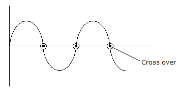
  9. Crossover distortion behaviour is characteristic of

  10. A.
    class A O/P stage
    B.
    class B O/P stage
    C.
    class AB output stage
    D.
    common pulse O/P state

  11. If aac for transistor is 0.98 then βac is equal to

  12. A.
    51
    B.
    49
    C.
    47
    D.
    45

  13. Assertion (A): The conductivity of p type semiconductor is higher than that of intrinsic semiconductor.

    Reason (R): The addition of donor impurity creates additional energy levels below conduction band.

  14. A.
    Both A and R are true and R is correct explanation of A
    B.
    Both A and R are true but R is not a correct explanation of A
    C.
    A is true but R is false
    D.
    A is false but R is true

  15. In an n-p-n transistor biased for operation in forward active region

  16. A.
    emitter is positive with respect to base
    B.
    collector is positive with respect to base
    C.
    base is positive with respect to emitter and collector is positive with respect to base
    D.
    none of the above

  17. An increase in temperature increases the width of depletion layer.

  18. A.
    True
    B.
    False

  19. A zener diode is used in

  20. A.
    voltage regulator circuit
    B.
    amplifier circuits
    C.
    both voltage regulator and amplifier circuit
    D.
    none of the above