Home / ECE / Electronic Devices and Circuits :: Section 2

ECE :: Electronic Devices and Circuits

  1. The drain characteristics of JFET in operating region, are

  2. A.
    inclined upwards
    B.
    almost flat
    C.
    inclined downwards
    D.
    inclined upwards or downwards

  3. As temperature increases

  4. A.
    the forbidden energy gap in silicon and germanium increase
    B.
    the forbidden energy gap in silicon and germanium decrease
    C.
    the forbidden energy gap in silicon decreases while that in germanium decreases
    D.
    the forbidden energy gap in silicon increases while that in germanium decreases

  5. When a reverse bias is applied to a p-n junction, the width of depletion layer.

  6. A.
    decreases
    B.
    increases
    C.
    remains the same
    D.
    may increase or decrease

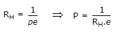
  7. The Hall constant in Si bar is given by 5 x 103 cm3/ coulomb, the hole concentration in the bar is given by

  8. A.
    105/cm3
    B.
    1.25 x 10¹⁵/cm3
    C.
    1.5 x 10¹⁵/cm3
    D.
    1.6 x 10¹⁵/cm3

  9. Which of the following devices has a silicon dioxide layer?

  10. A.
    NPN transistor
    B.
    Tunnel diode
    C.
    JFET
    D.
    MOSFET

  11. Which statement is false as regards holes

  12. A.
    Holes exist in conductors as well as semiconductors
    B.
    Holes constitute positive charges
    C.
    Holes exist only in semiconductors
    D.
    Holes and electrons recombine

  13. Photo electric emission can occur only if

  14. A.
    wave length of incident radiation is equal to threshold value
    B.
    wave length of incident radiation is less than threshold value
    C.
    frequency of incident radiation is less than threshold frequency
    D.
    none of the above

  15. The reverse saturation current of a diode does not depend on temperature.

  16. A.
    True
    B.
    False

  17. In a piezoelectric crystal, application of a mechanical stress would produce

  18. A.
    plastic deformation of the crystal
    B.
    magnetic Dipoles in the crystal
    C.
    electric polarization in the crystal
    D.
    shift in the Fermi level

  19. The value of a in a transistor

  20. A.
    is always equal to 1
    B.
    is less than 1 but more than 0.9
    C.
    is about 0.4
    D.
    is about 0.1