Home / ECE / Electronic Devices and Circuits :: Section 13

ECE :: Electronic Devices and Circuits

  1. How is an N-channel junction Field Effect Transistor operated as an amplifier?

  2. A.
    With a forward bias gate source junction
    B.
    With a reverse bias gate-source junction
    C.
    With a open gate source junction
    D.
    With a shorted gate source junction

  3. The Ebers-moll equation for IE in CB configuration is given by

  4. A.
    IE = anICIEC0
    B.
    IE = aIIC + IC0
    C.
    IE = anIC + IC0(eqVEB/KT-1)
    D.
    IE = aIIC + IE0(eqVEB/KT - 1)

  5. Ferrites are

  6. A.
    hard materials
    B.
    brittle materials
    C.
    not easily machinable
    D.
    materials with all above properties

  7. The merging of a hole and an electron is called

  8. A.
    recombination
    B.
    covalent bonding
    C.
    thermal union
    D.
    none of the above

  9. Which of the following semiconductor has the highest melting point?

  10. A.
    Germanium
    B.
    Silicon
    C.
    Gallium arsenide
    D.
    Lead sulphide

  11. The equivalent circuit of an ideal diode is

  12. A.
    a charging condenser
    B.
    a discharging condenser
    C.
    a switch
    D.
    a resistor

  13. What is meant by "continuous collector current" in BJT?

  14. A.
    Maximum collector current
    B.
    Current at Quiescent condition
    C.
    Leakage current
    D.
    Junction Capacitance charging and discharging current

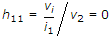
  15. The small signal input impedance of a transistor whose output is shorted for the measuring signal is


  16. Assertion (A): The frequency of light used for photoelectric emission is high.

    Reason (R): As per Einstein's equation 0.5 mv2 < hf - Uw.

  17. A.
    Both A and R are true and R is correct explanation of A
    B.
    Both A and R are true but R is not a correct explanation of A
    C.
    A is true but R is false
    D.
    A is false but R is true

  18. The electric breakdown strength is affected by

  19. A.
    shape of the waveform of applied voltage
    B.
    steepness of the wavefront of the applied voltage
    C.
    composition of the material
    D.
    all of the above