ECE :: Electronic Devices and Circuits
-
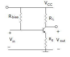
In the BJT amplifier shown in the figure is the transistor is biased in the forward active region. Putting a capacitor across RE will
-
In a centre tap full wave rectifier, 50 V is the peak voltage between the centre tap and one of the ends of the secondary. The maximum voltage across the reverse biased diode will be
-
Consider the following statements.
The functions of an oxide layer in an IC device is to- mask against diffusion or ion implant
- insulate the surface electrically
- increase the melting point of silicon
- produce a chemically stable protective layer of these statements.
-
If the gate of JFET is reverse biased, the width of depletion region
-
If the atomic number of germanium is 32, the number of electrons in the outer most shell will be
-
Dielectric loss due to polarisation occurs in
-
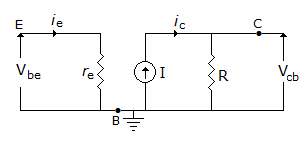
Figure shows small signal common base transistor circuit.The current source I and resistor R on the output side are
-
Consider the following statement associated with bipolar junction transistor and JFET
- The former has higher input impedance than the later
- The former has higher frequency stability than the later
- The later has lower noise figure than the former
- The later has higher power rating than the former.

 Whatsapp
 Facebook


 ie and re