ECE :: Analog Electronics
-
A radio frequency choke permits an easy flow of __________ current and at the same time it offers a very impedance to __________ currents.
-
Assertion (A): In an op-amp the gain bandwidth product equals ffinity
Reason (R): The change in open loop gain of an amplifier has almost no effect on closed loop gain
-
Lower chip area requirements of MOS is advantage in
-
For high frequency response of a transistor amplifier, suitable model to use is
-
Harmonic distortion in CB amplifier may be least when the load resistance is
-
If a common emitter amplifier with an emitter resistance RC has an overall transconductance gain of 1 m A/V, a voltage gain of - 4 and desensitivity of 50, then the value of the emitter resistance R would be
-
Turn on time of a transistor switch is equal to sum of (where tr is rise time, td is delay time)
-
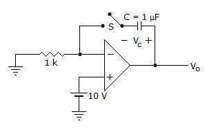
For the circuit shown in the figure, the capacitor C is initially uncharged. At t = 0, the switch S is closed. The voltage Vc across the capacitor at t = 1 millisecond is (In the figure shown above, the op-amp is supplied with ± 15 V and the ground has been shown by the symbol)
-
In amplifiers, the parasitic oscillation result due to

 Whatsapp
 Facebook

