Home / ECE / Analog Electronics :: Section 15

ECE :: Analog Electronics

  1. Assertion (A): Manufacturer's quote h parameters of transistor

    Reason (R): h parameters of a transistor are easiest to measure

  2. A.
    Both A and R are correct and R is correct explanation for A
    B.
    Both A and R are correct but R is not correct explanation for A
    C.
    A is correct R is wrong
    D.
    A is wrong R is correct

  3. The P-type substrate in a conventional pn Junction isolated integrated circuits should be connected to

  4. A.
    any where
    B.
    a dc ground potential
    C.
    the most positive potential available in the circuit
    D.
    the most negative potential available in the circuit

  5. Wien bridge uses

  6. A.
    lead network
    B.
    lag network
    C.
    lead-lag network
    D.
    Both (a) and (b)

  7. Which of the following is not necessarily the advantages of a push pull amplifier?

  8. A.
    It gives more output
    B.
    It removes odd a well as even harmonics
    C.
    There is no effect of ripple of the power supply
    D.
    It consumes least power

  9. Which of the following best represents the output impedance of an actual op-amp?

  10. A.
    10 ohm
    B.
    100 ohm
    C.
    10 k ohm
    D.
    100 k ohm

  11. In CE amplifier

  12. A.
    input and output are in phase
    B.
    phase difference between input and output is 30° to 90°
    C.
    phase difference between input and output is 60° to 120°
    D.
    output is inverted with respect to its input voltage

  13. The approximate value of input impedance of a common emitter amplifier with emitter resistance Re is given by

  14. A.
    hie + AI Re
    B.
    hie + (i + hfe) Re
    C.
    hie
    D.
    (1 + hfe) Re

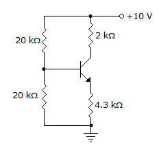
  15. The collector voltage VC of the circuit shown in the given figure aside is approximately

  16. A.
    2 V
    B.
    4.6 V
    C.
    8 V
    D.
    8.6 V

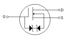
  17. The symbol shown in figure represents a

  18. A.
    P-channel MOSFET
    B.
    UJT with N-type base
    C.
    N-channel DEMOSFET with internal zener protection
    D.
    P-channel DEMOSFET with internal zener protection

  19. The phase angle of a lag circuit is

  20. A.
    between 0 and -90°
    B.
    between 0 and +90°
    C.
    90°
    D.
    more than 90°