ECE :: Analog Electronics
-
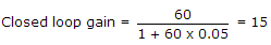
It is desired to reduce distortion in an amplifier from 8% to 2% by using 5% negative feedback. The open and closed loop gains respectively are
-
An ideal op-amp requires
-
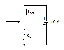
The JFET in the circuit shown in figure has an IDSS = 10 mA and Vp = -5V. The value of the resistance Rs for a drain current IDS = 6.4 mA is
-
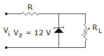
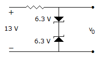
In figure the zener has a resistance of 5 ohms. As the load resistance is varied, the output voltage
-
Percentage increase in the reverse saturation current of a diode if the temperature is increased from 25°C to 50°C
-
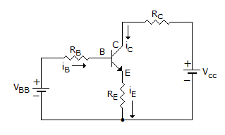
The transistor of following figure in Si diode with a base current of 40 μA and ICBO = 0, if VBB = 6V, RE = 2 kΩ and β = 90, IBQ = 20 μA then IEQ =
-
In a self bias circuit for CE amplifier, an increase in emitter resistance RE results in

 Whatsapp
 Facebook


 .
.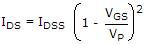
 VGS = - 1 V
 .
.
 = 2(T2 - T1)/10
 , ICQ = β IBQ = 90 x 20 μA = 1800 μA.