ECE :: Analog Electronics
-
Assertion (A): An op-amp has high voltage gain, high input impedance and low output impedance
Reason (R): Negative feedback increases output impedance
-
A transistor has a maximum power dissipation of 350 mW at an ambient temperature of 25°C. If derating factor is 2 mW/°C, the maximum power dissipation for 40°C ambient temperature is
-
The output voltage waveform of a CE amplifier is fed to a dc coupled CRO. The trace on the screen will be
-
In an RC phase shift oscillator, the total phase shift of the three RC lead networks is
-
In the circuit of figure β = 100 and quiescent value of base current is 20 μA. The quiescent value of collector
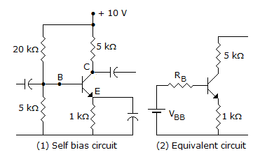 current is
 -
Assertion (A): In an op-amp the voltage gain and band width can be adjusted as per requirement
Reason (R): Large value capacitor can also be fabricated on a chip
-
In figure which diode will conduct and what will be the value of V0?

-
For the amplifier circuit of figure, the h parameters of transistor are hib = 25 Ω, hfb = 0.999, hob = 10-6 Ω. The voltage gain is

-
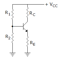
In figure, VCC = + 30 V, R1 = 200 kΩ and R2 = 100 kΩ. If VBE = 0.7 V, the voltage a cross RE =

 Whatsapp
 Facebook


 .
. .
. .
.