Home / ECE / Analog Electronics :: Section 13

ECE :: Analog Electronics

  1. In a common Emitter BJT amplifier, the maximum usable supply voltage is limited by

  2. A.
    avalanche breakdown of Base emitter junction
    B.
    collector to Base Breakdown voltage with emitter open (βVCBO)
    C.
    collector Emitter Breakdown voltage with base open (βVCBO)
    D.
    zener breakdown voltage of the emitter base Junction

  3. High frequency oscillations can be caused by

  4. A.
    electric coupling
    B.
    magnetic coupling
    C.
    ground loop
    D.
    all of the above

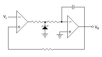
  5. In order to obtain triangular pulses at the output of the circuit in the figure, the input should be.
  6. A.
    grounded
    B.
    a square wave
    C.
    Triangular wave
    D.
    Trigger

  7. The circuit in figure is

  8. A.
    rectifier
    B.
    voltage to frequency converter
    C.
    frequency to voltage converter
    D.
    logarithmic amplifier

  9. A feedback network to be used with an amplifier to provide oscillation is tested and found to give an output of 0.124 V with a 0.5 V input. What will be the effect on output if the amplifier's gain is twice that required by the Barkhausen criterion?

  10. A.
    Linear oscillations
    B.
    Non-linear oscillations
    C.
    Damped oscillations
    D.
    No oscillations

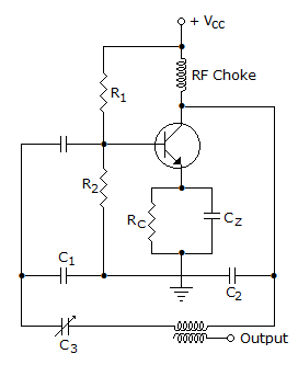
  11. The oscillator shown in figure is a

  12. A.
    Clapp oscillator
    B.
    R-C Phase shift oscillator
    C.
    Hartley oscillator
    D.
    Colpitt's oscillator

  13. In a combination limiter with sinusoidal input voltage the output wave can be nearly square.

  14. A.
    True
    B.
    False

  15. Assertion (A): A Darlington amplifier has very low output impedance

    Reason (R): The circuit has a low resistance RE between emitter and ground

  16. A.
    Both A and R are correct and R is correct explanation for A
    B.
    Both A and R are correct but R is not correct explanation for A
    C.
    A is correct R is wrong
    D.
    A is wrong R is correct

  17. A Hartley oscillator uses

  18. A.
    a tapped inductor
    B.
    a tapped capacitor
    C.
    both (a) and (b)
    D.
    neither (a) nor (b)

  19. A silicon PN junction diode under reverse bias has depletion region of width 10 μm. The relative permittivity of silicon, εr = 11.7 and the permittivity of free space ε0 = 8.85 x 10⁻¹² F/m. The depletion capacitance of the diode per square meter is

  20. A.
    100 μF
    B.
    10 μF
    C.
    1 μF
    D.
    20 μF