Home / ECE / Digital Electronics :: Section 7

ECE :: Digital Electronics

  1. TTL logic is preferred to DRL logic because

  2. A.
    greater fan-out is possible
    B.
    greater logic levels are possible
    C.
    greater fan-in is possible
    D.
    less power consumption is achieve

  3. Assertion (A): Schottky transistors are preferred over normal transistors in digital circuits

    Reason (R): A Schottky transistor when used as a switch, between cutoff and active region.

  4. A.
    Both A and R are correct and R is correct explanation of A
    B.
    Both A and R are correct but R is not correct explanation of A
    C.
    A is true, R is false
    D.
    A is false, R is true

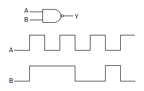
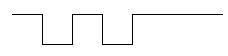
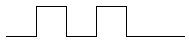
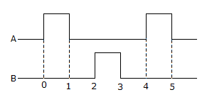
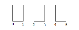
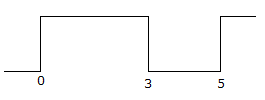
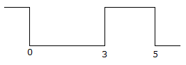
  5. The inputs A and B of the given figure are applied to a two input NOR gate. The output waveform is


  6. A parallel in-parallel out shift register can be used to introduce delay in digital circuits.

  7. A.
    True
    B.
    False

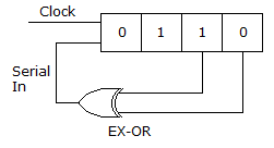
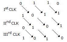
  8. In following figure, the initial contents of the 4-bit serial in parallel out, right shift, shift register as shown in figure are 0110. After 3 clock pulses the contents of the shift register will be

  9. A.
    0000
    B.
    0101
    C.
    1010
    D.
    1110

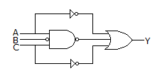
  10. For the logic circuit of the given figure, the minimized expression is

  11. A.
    B.
    Y = A + B + C
    C.
    Y = A + B
    D.
    Y = ABC

  12. Binary multiplication can be done by repeated addition.

  13. A.
    True
    B.
    False

  14. Assertion (A): In totem pole output the output impedance is low.

    Reason (R): TTL gate with active pull up should not be used in wired AND connection.

  15. A.
    Both A and R are correct and R is correct explanation of A
    B.
    Both A and R are correct but R is not correct explanation of A
    C.
    A is true, R is false
    D.
    A is false, R is true

  16. A 4 bit synchronous counter uses flip flops with a delay time of 15 ns each. The time required for change of state is

  17. A.
    15 ns
    B.
    30 ns
    C.
    45 ns
    D.
    60 ns

  18. The inputs to a NAND gate are as shown in the given figure. The waveform of output is