ECE :: Exam Questions Paper
-
An average response rectifier type electronic voltameter has a d.c. voltage of 10 V applied to it. What is the meter reading?
-
Consider the common emitter amplifier shown below with the following circuit parameters: β = 100, gm = 0.3861 A/V, r0 = ∞ rp = 259 Ω, Rs = 1 kΩ, RB = 93 kΩ, RC = 250 Ω, RL = 1 kW, C1 = ∞ and C2 = 4.7mF.
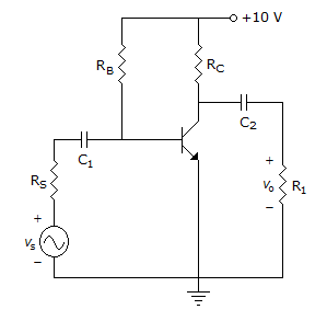
The lower cut-off frequency due to C2 is -
Number of fundamental cut-sets of any graph will be
-
Consider a silicon p-n junction at room temperature having the following parameters:
Doping on the n-side = 1 x 1017 cm-3
Depletion width on the n-side = 0.1 μm
Depletion width on the p-side = 1.0 μm
Intrinsic carrier concentration = 1.4 x 10¹⁴F. cm-1.
Thermal voltage = 26mV
Permittivity of free space = 8.85 x 10⁻¹⁴F. cm-1.
Dielectric constant of silicon = 12. A built in potential of the junction. -
A message signal x(t) is amplitude modulated with carrier c(t).
x(t) = 2 sin 600pt
c(t) = 8 cos (2p x 106 t)
such that the modulated signal is
(8 + 2 sin 600pt) [cos 2p x 106 t]
The total side band power is: -
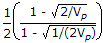
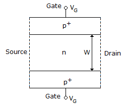
The cross section of a JFET is shown in the following figure. Let Va be - 2 V and let Vp be the initial pinch-off voltage. If the width W is doubled (with other geometrical parameters and doping levels remaining the same), then the ratio between the mutual transconductances of the initial and the modified JFET is
-
A 2 μF capacitor is shunted by a 1 kΩ maintained at temperature 400 K. The rms noise voltage across the capacitor over the entire frequency band is:

 Whatsapp
 Facebook