Home / ECE / Analog Electronics :: Section 20

ECE :: Analog Electronics

  1. CMRR of an op-amp is about 0.1.

  2. A.
    True
    B.
    False

  3. A transistor amplifier has poles at
    s1 = - 0.000245 x 10⁹ rad/sec.
    s2 = - 0.0748 x 10⁹ rad/sec.
    s3 = - 0.670 x 10⁹ rad/sec.
    s4 = - 4.38 x 10⁹ rad/sec.
    The upper 3 dB frequency of the amplifier will be

  4. A.
    s1
    B.
    s1 + s2 + s3 + s4
    C.
    s1 + s4
    D.
    s4

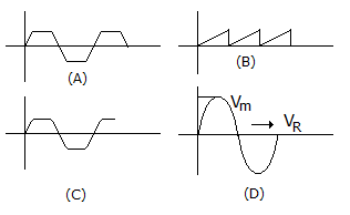
  5. In the circuit of figure for sinusoidal input the waveform of the output will be as shown in

  6. A.
    figure A
    B.
    figure B
    C.
    figure C
    D.
    figure D

  7. An engineer designs an amplifier to have a voltage gain of 60, but when constructed it only had a gain of 50. What value of feedback will double the gain?

  8. A.
    +0.5%
    B.
    +0.66%
    C.
    +1%
    D.
    +3.3%

  9. The maximum theoretical efficiency for class A amplifier is

  10. A.
    12.5%
    B.
    25%
    C.
    50%
    D.
    75%

  11. In the case of an amplifier, the normalised voltage gain is given by.

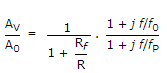
    where f0 is zero frequency, fP is pole frequency. For a standard frequency response of the amplifier,

  12. A.
    fP >> f0
    B.
    fP = f0
    C.
    fP << f0
    D.
    f0 = 2 fP

  13. In a rectifier only a portion of input power is converted into DC power. The rest is AC power.

  14. A.
    True
    B.
    False

  15. The slope of the transfer characteristics of an N-channel JFET is

  16. A.
    positive
    B.
    negative
    C.
    constantly varying
    D.
    zero

  17. Figure shows a

  18. A.
    bipolar transistor
    B.
    JFET
    C.
    p-channel MOSFET
    D.
    n-channel enhancement MOSFET

  19. In a current mirror

  20. A.
    the i - v curve of compensating diode is similar to collector curve of transistor
    B.
    the i - v curve of compensating diode is similar to transconductance curve of transistor
    C.
    either (a) or (b)
    D.
    neither (a) nor (b)