Home / ECE / Analog Electronics :: Section 20

ECE :: Analog Electronics

  1. In a CE amplifier it is desired that the signal should be able to swing equally in both directions. Then the Q point should be

  2. A.
    at the centre of ac load line
    B.
    at the centre of dc load line
    C.
    at the centre of collector voltage
    D.
    at the centre of collector current

  3. In a base driver amplifier the voltage gain is the ratio of

  4. A.
    ac collector voltage to ac base voltage
    B.
    ac emitter voltage to ac base voltage
    C.
    ac collector voltage to ac emitter voltage
    D.
    ac base voltage to ac emitter voltage

  5. Assertion (A): A class C amplifier is a timed amplifier which needs a tank circuit as the load in the collector circuit of the transistor for its proper operation

    Reason (R): In class C operation collector current flows for less than 180° of the ac cycle and thus flows in pulses

  6. A.
    Both A and R are correct and R is correct explanation for A
    B.
    Both A and R are correct but R is not correct explanation for A
    C.
    A is correct R is wrong
    D.
    A is wrong R is correct

  7. A junction Field Effect Transistor can operate in

  8. A.
    depletion mode only
    B.
    enhancement mode only
    C.
    depletion and enhancement modes
    D.
    neither depletion nor enhancement modes

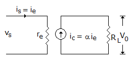
  9. The re model equivalent circuit shown in figure is for

  10. A.
    CE amplifier
    B.
    CC amplifier
    C.
    CB amplifier
    D.
    None of the above

  11. CMRR is the ratio of differential voltage gain to common mode gain.

  12. A.
    True
    B.
    False

  13. The purpose of impedance matching in an amplifier circuit is to achieve

  14. A.
    high efficiency
    B.
    reduce distortion
    C.
    maximum power transfer
    D.
    none of the above

  15. For the circuit of figure the input and output Miller resistances are

  16. A.
    5 kΩ each
    B.
    1 ohm and 5 kΩ respectively
    C.
    5 kΩ and 1 ohm respectively
    D.
    1 ohm each

  17. In a BJT CE amplifier circuit the value of coupling capacitor should be such that

  18. A.
    its reactance is small for the lowest frequency in the input and output
    B.
    its reactance is high for the lowest frequency in the input and output
    C.
    its reactance is zero for the lowest frequency in the input and output
    D.
    its reactance is infinite for the lowest frequency in the input and output

  19. In order to rectify sinusoidal signals of millivolt range (< 0.6 V)

  20. A.
    bridge rectifier using diodes can be employed
    B.
    full wave diode rectifier can be used
    C.
    a diode is to be inserted in the feedback loop of an op-amp
    D.
    a diode is to be inserted in the I/P of an op-amp