Home / ECE / Analog Electronics :: Section 20

ECE :: Analog Electronics

  1. The common gate amplifier has a characteristically __________ input resistance and a __________ output resistance.

  2. A.
    low, low
    B.
    high, high
    C.
    low, high
    D.
    high, low

  3. For input and later stages, BI-FET op-amp use

  4. A.
    JFETs and MOSFETs respectively
    B.
    MOSFETs and JFETs respectively
    C.
    JFETs and BJTs respectively
    D.
    BJTs and JFETs respectively

  5. The emitter coupled pair of BJT's gives a linear transfer relation between the differential output voltage and the differential input voltage Vid only when the magnitude of Vid is less a times the thermal voltage, where a is

  6. A.
    4
    B.
    3
    C.
    2
    D.
    1

  7. In most transistor the collector region is made physically larger than the emitter region

  8. A.
    for dissipating heat
    B.
    to distinguish it from other regions
    C.
    as it is sensitive to ultraviolet rays
    D.
    to reduce resistance in the path of flow of electrons

  9. The leakage current in CB configuration may be around

  10. A.
    few micro amperes
    B.
    few hundred micro amperes
    C.
    few milliamperes
    D.
    few hundred milliamperes

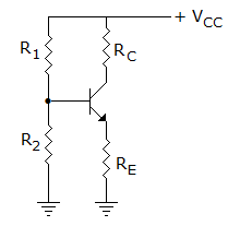
  11. In figure VCC = + 30 V, IC corresponding to Q point is 1 mA. If RC = 5 kΩ and RE = 5 kΩ, VCE corresponding to Q point is

  12. A.
    30 V
    B.
    20 V
    C.
    25 V
    D.
    5 V

  13. Symbol shown in figure represents a

  14. A.
    Enhancement only N-channel MOSFET
    B.
    UJT with p-type base
    C.
    N-channel DMOSFET with internal protection
    D.
    Phototransistor

  15. In which of the following circuits is op-amp used in open loop configuration?

  16. A.
    Comparator
    B.
    Summing amplifier
    C.
    Integrating amplifier
    D.
    Logarithmic amplifier

  17. In the op-amp circuit of figure, V0 =

  18. A.
    3 V1 - 4 V2
    B.
    -3 V1 + 4 V2
    C.
    3(V1 - V2)
    D.
    -3(V1 - V2)

  19. In a diode rectifier with a capacitance input filter, a surge current is likely to flow when the circuit is switched on. The cause of this surge current is

  20. A.
    the non linear behaviour of diodes
    B.
    the capacitor acts as a short circuit at the instant of switching,
    C.
    the inductance of leads
    D.
    both (a) and (b)