GATE 2017-2018 :: GATE Instrumentation
- Signals from fifteen thermocouples are multiplexed and each one is sampled once per second with a 16-bit ADC. The digital samples are converted by a parallel to serial converter to generate a serial PCM signal. This PCM signal is frequency modulated with FSK modulator with 1200 Hz as 1 and 960 Hz as 0. The minimum band allocation required for faithful reproduction of the signal by the FSK receiver without considering noise is
-
Three capacitors C1, C2 and C3 whose values are 10μF,5μF, and 2μF respectively, have breakdown voltages of 10V, 5V, and 2V respectively. For the interconnection shown below, the maximum safe voltage in Volts that can be applied across the combination, and the corresponding total charge in μC stored in the effective capacitance across the terminals are, respectively,

- The maximum value of the solution y (t) of the differential equation y(t) + ӱ(t) = 0 with initial conditions ӱ(0) = 1 and y(0) = 1, for t ≥ 0 is
-
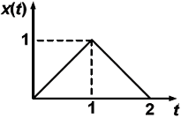
The Laplace Transform representation of the triangular pulse shown below is
-
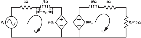
In the circuit shown below, if the source voltage VS = 100∠53.13o Volts, then the Thevenin's equivalent voltage in Volts as seen by the load resistance RL is
-
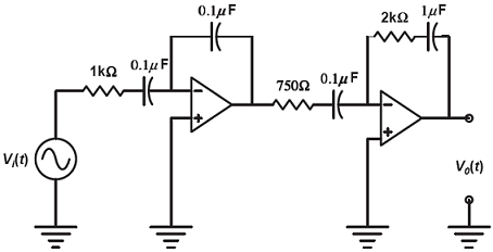
A signal Vi (t) = 10 +10 sin100 πt + 10sin 4000 πt + 10sin100000 πt is supplied to a filter circuit (shown below) made up of ideal op-amps. The least attenuated frequency component in the output will be
-
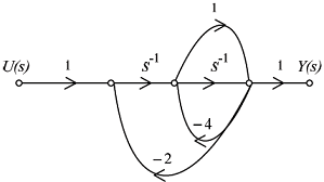
The signal flow graph for a system is given below. The transfer function Y(s)/U(s) for this system is given as
-
A voltage 1000 sin wt Volts is applied across YZ. Assuming ideal diodes, the voltage measured across WX in Volts, is

-
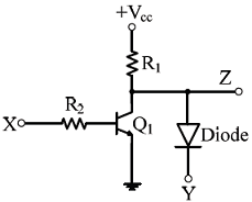
In the circuit shown below, Q1 has negligible collector-to-emitter saturation voltage and the diode drops negligible voltage across it under forward bias. If Vcc is +5 V, X and Y are digital signals with 0 V as logic 0 and Vcc as logic 1, then the Boolean expression for Z is

 Whatsapp
 Facebook


 .
. .
. .
.