Discussion :: GATE ECE
-
In the three dimensional view of a silicon n-channel MOS transistor shown below, δ = 20 nm. The transistor is of width 1 μm. The depletion width formed at every p-n junction is 10 nm. The relative permitivities of Si and SiO2 respectively, are 11.7 and 3.9, and ε0 = 8.9 * 10-12 F/m.
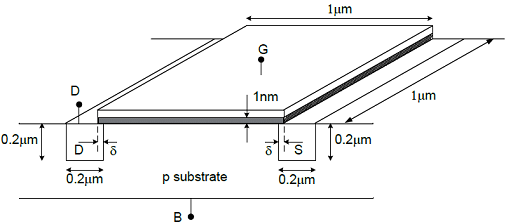 The gate-source overlap capacitance is approximately

 Whatsapp
 Facebook


Answer : Option A
Explanation :
-NA-
Be The First To Comment