Home / ECE / Analog Electronics :: Section 11

ECE :: Analog Electronics

  1. Which of the amplifier circuits using junction transistors has the best gain?

  2. A.
    Common emitter
    B.
    Common base
    C.
    Common collector
    D.
    All above has the same gain

  3. To obtain very high input and O/P impedance in a feedback amplifier, the type of feedback utilized

  4. A.
    voltage series
    B.
    current series
    C.
    voltage shunt
    D.
    current shunt

  5. The thermal resistance of a BJT is about

  6. A.
    100° C/W
    B.
    200° C/W
    C.
    20° C/W
    D.
    2° C/W

  7. Oscillator with best frequency stability is

  8. A.
    Crystal oscillator
    B.
    Phase shift oscillator
    C.
    Clapp oscillator
    D.
    Hartley oscillator

  9. The IF amplifier in a superheterodyne receiver is

  10. A.
    single-stage single-timed amplifier
    B.
    two stage of single tuned amplifier
    C.
    double tuned amplifier
    D.
    class-C amplifier

  11. Examine the circuit of figure and the following statements

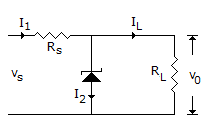
    1. Vs is more than the zener breakdown voltage.
    2. IL = I1 - I2.
    3. Rs is less than zener nominal resistance.
    Which of the above statements are correct?

  12. A.
    1, 2, 3
    B.
    1, 2
    C.
    1 only
    D.
    2 and 3

  13. The approximate value of input impedance of CE amplifier with emitter resistance RE is given by

  14. A.
    hie + Ai RE
    B.
    hie + (1 + hfe) RE
    C.
    hie
    D.
    (1 + hfe) RE

  15. The advantage of using crystal oscillator is that it

  16. A.
    requires low d.c. supply voltage
    B.
    works at high frequency
    C.
    gives high output voltage
    D.
    gives constant frequency of oscillations

  17. A transistor will operate in inverted region when

  18. A.
    emitter junction is forward biased and collector junction is reverse biased
    B.
    emitter junction is reverse biased and collector junction is forward biased
    C.
    emitter junction as well as collector junction are forward biased
    D.
    emitter junction as well as collector junction are reverse biased

  19. Cross-over distortion behaviour is a characteristic of

  20. A.
    class A output stage
    B.
    class B output stage
    C.
    class AB output stage
    D.
    common base output stage