ECE :: Analog Electronics
-
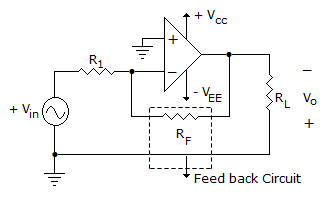
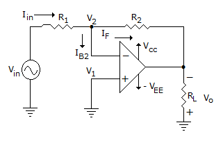
The feedback technique employed in the following circuit is
-
A second order active bandpass filter can be obtained by cascading LP second order filter having higher cut off frequency fOH with a second order HP filter having lower cut off frequency fOL provided
-
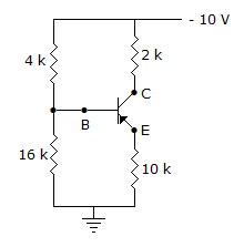
In figure the approximate voltages of
-
The open loop gain of an amplifier is 50 but likely to decrease by 20% due to various factors. If negative feedback with β = 0.1 is used, the change in gain will be about
-
An increase in ambient temperature means that maximum power rating of transistor
-
Two CE stages are coupled through a capacitor. To calculate the quiescent base current of the two transistors, the capacitor is treated as
-
If it is desired to have low output impedance in an amplifier circuit then we should use
-
Generally the gain of a transistor amplifier falls at high frequencies due to the

 Whatsapp
 Facebook


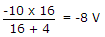 . Emitter voltage = - 8 + 0.7 = - 7.3 V.